ALLPCB


When designing and producing printed circuit boards (PCBs), two critical factors that can make or break the performance and reliability of your project are total PCB thickness and warpage issues. These elements directly impact the assembly process, component compatibility, and long-term durability of the board, especially when using materials like FR-4 or components such as Ball Grid Arrays (BGAs). In this comprehensive guide, we’ll dive deep into how PCB thickness and warpage affect design and production, offering practical solutions for engineers working on complex projects.
Why PCB Thickness and Warpage Matter in Design and Production
PCB thickness and warpage are not just minor details; they are fundamental to ensuring a board functions as intended. Thickness determines mechanical stability, compatibility with enclosures, and even signal integrity in high-speed applications. Warpage, on the other hand, refers to the unintended bending or twisting of the board, which can lead to soldering defects, component misalignment, and even complete failure during assembly or operation.
For designs involving FR-4 material—a common choice due to its cost-effectiveness and versatility—and BGA components, which require precise placement and soldering, controlling thickness and minimizing warpage are non-negotiable. Let’s explore these challenges in detail and provide actionable insights for your next PCB design and PCB production project.
Understanding Total PCB Thickness
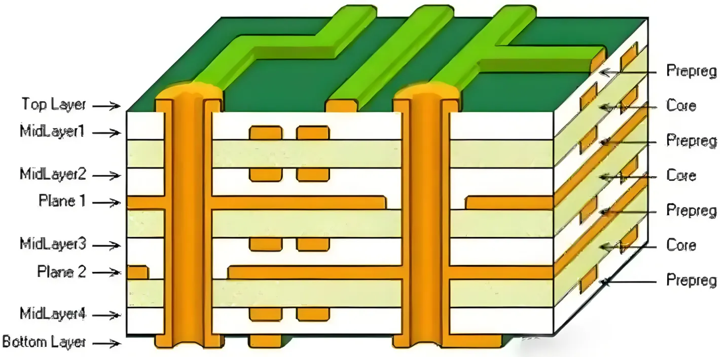
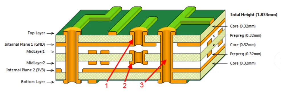
The total thickness of a PCB is determined by the number of layers, the thickness of the core material, prepreg (pre-impregnated resin layers), and copper foil used in its construction. Standard thicknesses range from 0.4 mm for ultra-thin boards to 3.2 mm or more for heavy-duty applications. For most consumer electronics using FR-4, a thickness of 1.6 mm is common, providing a balance of durability and flexibility.
Thickness directly impacts several aspects of PCB production:
- Mechanical Strength: Thicker boards are more robust and less prone to bending under stress, which is crucial for applications with heavy components or high vibration environments.
- Thermal Management: Thicker boards can dissipate heat better, which is essential for high-power designs.
- Signal Integrity: In multilayer boards, thickness affects impedance control. For instance, maintaining a 50-ohm impedance for high-speed signals requires precise dielectric thickness between layers, often in the range of 0.1 to 0.2 mm per layer for FR-4 material.
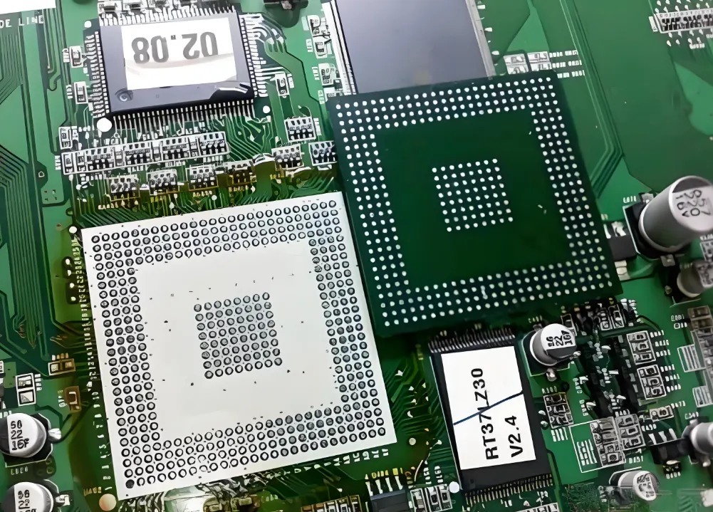
- Component Compatibility: BGA components, with their dense pin arrays, often require specific board thicknesses to ensure proper soldering and heat distribution during reflow processes.
How to Choose the Right PCB Thickness
Selecting the appropriate thickness for your board depends on your project requirements. Here are some guidelines:
- Application Needs: For lightweight, portable devices, opt for thinner boards (0.8–1.2 mm). For industrial equipment, consider thicker boards (2.0–3.2 mm) to handle mechanical stress.
- Layer Count: More layers mean increased thickness. A 4 layer board might be around 1.6 mm, while an 8-layer board could reach 2.4 mm or more with standard FR-4 material.
- Component Constraints: BGA components often require a minimum thickness to avoid excessive flexing during assembly, typically 1.6 mm or higher, to prevent solder joint failures.
Work closely with your manufacturing partner to finalize the stack-up and ensure the chosen thickness aligns with both design and production capabilities.
What Causes PCB Warpage and Why It's a Problem
Warpage is the deformation of a PCB, where the board deviates from being perfectly flat. This issue can occur during manufacturing, assembly, or even in the field due to environmental factors. Warpage is particularly problematic in BGA component PCB designs, as even a slight deviation (as little as 0.1 mm across a 100 mm board) can lead to poor solder connections or component misalignment.
Common causes of warpage include:
- Material Mismatch: FR-4 material consists of woven fiberglass and epoxy resin, which expand and contract at different rates when exposed to heat. This mismatch, especially during the reflow soldering process (which can reach temperatures of 260°C), often causes bending.
- Uneven Copper Distribution: If one side of the board has significantly more copper than the other, the imbalance can create stress, leading to warpage. For instance, a board with a dense ground plane on one layer and sparse traces on another is at risk.
- Improper Stack-Up Design: In multilayer boards, an asymmetrical stack-up (e.g., unequal dielectric thicknesses or unbalanced copper layers) can induce stress during lamination.
- Thermal Stress: Repeated heating and cooling cycles during assembly or operation can exacerbate warpage, especially in boards with high component density like those using BGA packages.
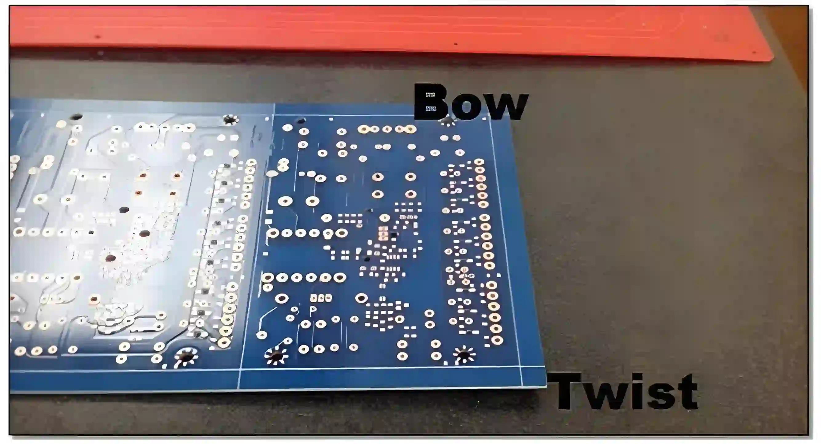
Impact of Warpage on PCB Production and Assembly
Warpage creates significant challenges during PCB production and assembly:
- Soldering Defects: For BGA components, warpage can prevent uniform contact between the solder balls and pads, leading to open circuits or weak joints. Studies suggest that warpage beyond 0.75% of the board’s diagonal length can cause assembly failures.
- Component Misalignment: Automated pick-and-place machines rely on a flat surface. Warped boards can result in misplaced components, increasing rework costs.
- Testing Issues: Warped boards may not fit properly into testing fixtures, leading to inaccurate results or delays in validation.
Solutions to Minimize PCB Thickness and Warpage Issues
Addressing thickness and warpage challenges requires careful planning during the PCB design phase and collaboration during production. Here are proven strategies to ensure success:
Optimizing PCB Thickness
Balancing thickness for functionality and manufacturability is key. Consider these tips:
- Standardize Where Possible: Stick to common thicknesses like 1.6 mm for FR-4 boards unless your design specifically requires otherwise. This reduces production complexity and cost.
- Simulate Stack-Up Early: Use design software to simulate the stack-up and verify impedance values. For high-speed signals, ensure dielectric layers maintain consistent thickness (e.g., 0.15 mm between signal and ground planes for 50-ohm impedance).
- Account for BGA Requirements: Ensure the board is thick enough to handle thermal expansion during soldering. A 1.6–2.0 mm thickness often works well for BGA designs.
Preventing Warpage in Design and Production
Warpage can often be mitigated with thoughtful design and manufacturing practices:
- Balance Copper Distribution: Ensure copper layers are as symmetrical as possible. If a ground plane occupies 80% of one layer, try to match that coverage on the opposite layer to reduce stress.
- Symmetrical Stack-Up: Design multilayer boards with a balanced stack-up. For example, in a 6-layer board, place signal layers and planes symmetrically around the core to minimize internal stresses.
- Control Thermal Profiles: During production, use a gradual heating and cooling profile in the reflow oven to avoid sudden thermal shocks. A peak temperature of 245–260°C for lead-free soldering, with a slow ramp-up of 1–3°C per second, can help.
- Use Panelization Techniques: During manufacturing, panelize boards with balanced designs to distribute stress evenly across the panel. Adding dummy copper fills in empty areas can also help.
- Reinforce with Stiffeners: For thin boards prone to bending, consider adding stiffeners or mounting hardware to maintain flatness during assembly.
Special Considerations for FR-4 Material and BGA Components
When working with FR-4 material and BGA component PCB designs, extra care is needed to address thickness and warpage:
FR-4 Material Properties
FR-4 is a composite material made of woven fiberglass and epoxy resin, widely used for its affordability and decent electrical properties. However, its coefficient of thermal expansion (CTE) is relatively high (around 14–17 ppm/°C in the X-Y direction), making it susceptible to warpage under thermal stress. To counter this:
- Choose high-Tg (glass transition temperature) FR-4 variants for better thermal stability, especially for lead-free soldering processes. A Tg of 170°C or higher is ideal for demanding applications.
- Avoid excessive moisture absorption during storage, as it can worsen warpage. Store boards in a controlled environment with humidity below 50%.
BGA Component Challenges
BGA components, with their dense array of solder balls (often 0.5–1.0 mm pitch), are highly sensitive to board flatness. Warpage as small as 0.2 mm can cause solder joint failures. To mitigate risks:
- Ensure precise coplanarity during design and assembly. Industry standards often recommend warpage limits of less than 0.75% of the board’s diagonal length for BGA packages.
- Use underfill materials post-soldering to reinforce BGA joints and reduce stress from thermal cycling.
- Verify reflow profiles to prevent uneven heating, which can exacerbate warpage under BGA areas.
Partnering for Success in PCB Production
Navigating the complexities of PCB thickness and warpage requires expertise and collaboration. Working with a reliable manufacturing partner ensures that your design is optimized for production. From stack-up validation to controlled thermal profiles during assembly, a skilled team can help you avoid costly mistakes and achieve high-quality results.
During the PCB production phase, ensure that your partner adheres to strict quality standards, such as IPC-6012 for rigid PCBs, which specifies acceptable warpage limits (typically 0.75–1.5% depending on board type). Request detailed feedback on stack-up designs and warpage measurements post-production to refine future projects.
Conclusion: Mastering PCB Thickness and Warpage for Reliable Designs
In the world of PCB design and PCB production, controlling total PCB thickness and warpage is essential for creating reliable, high-performing boards. Whether you’re using FR-4 material or integrating BGA components, understanding the interplay of design choices, material properties, and manufacturing processes can save time, reduce costs, and improve outcomes.
By optimizing thickness for your application, balancing copper distribution, and adhering to best practices during production, you can minimize warpage and ensure successful assembly. Remember to leverage simulation tools, collaborate with manufacturing experts, and prioritize quality at every stage of your project. With these strategies, you’re well-equipped to tackle the challenges of modern PCB design and deliver exceptional results.